Advanced Functional Materials

The research aims to explore and develop an original approach for the growth of sustainable functional oxide thin films for electronic and optical applications. We intend to demonstrate that by a precise control of the nature and concentration of dopants and structural defect density it is possible to tune the physical properties of oxide thin films and to give them new functionalities. The PCAFM Group employs a range of techniques including pulsed electron beam deposition method (PED), evaporation, sputtering and characterization for the study of thin film growth and the structure-function relationships in sustainable materials.
PED method for thin film growth 

We have built-up and optimized a pulsed electron beam source for the growth of thin films by ablation (the pulsed electron beam deposition method, PED). This growth technique has features similar with the pulsed laser deposition (PLD) but uses a pulsed electron beam instead of a laser beam. The PED method has the advantage to grow oxide thin films with a very good control of the surface morphology, cationic composition, oxygen stoichiometry and crystalline structure of the films.

Epitaxial oxide thin films  

Epitaxial oxide thin films were grown by PED on single crystal substrates leading to films with different functional physical properties. As example, epitaxial indium oxide films with the cubic bixbyite structure obtained by PED on c-cut sapphire substrates revealed two distinct structural phases in the films: an ordered bixbyite phase with the three-fold symmetry in the (111) plane, and a disordered bixbyite phase with a six-fold symmetry in the (111) plane. This large disorder in the oxygen network of In2O3 films maintained the high optical transparency but tailored the electrical properties.

Metal-insulator transition (MIT)   

Epitaxial undoped ZnO thin films have been grown on Al2O3 single crystal substrates by PED in the 300° - 450°C range with a metallic conductivity at room temperature followed by a MIT at about 150 K. Such a behavior has been already observed in ZnO films doped by various elements (Al, Ga, Ti B, etc.), but for the first time in pure ZnO films. The transport properties have been changed from a classical semiconductor behavior to a degenerate semiconductor with MIT due to a small variation in the oxygen pressure during the growth of epitaxial In2O3 thin films by PED. MIT was observed at low temperatures in Ti based oxide films (La2/3TiO3-δ, SrTiO3- δ, Ba0.2Sr0.8TiO3- δ) grown by PLD due to the effects of oxygen deficiency (i.e. about 15% of oxygen missing).

MIT in ZnO thin films

Multifunctional zinc oxide thin films   

The research covered fundamental science related to thin film composition and structure and applied research through “passive” or “active” properties of thin films. Nd-doped ZnO films were grown with highly tunable properties, from transparent conducting oxide (“passive films”) to photon down-shifting thin films (“active” films) for solar cells.

Nanocomposite oxide thin films   

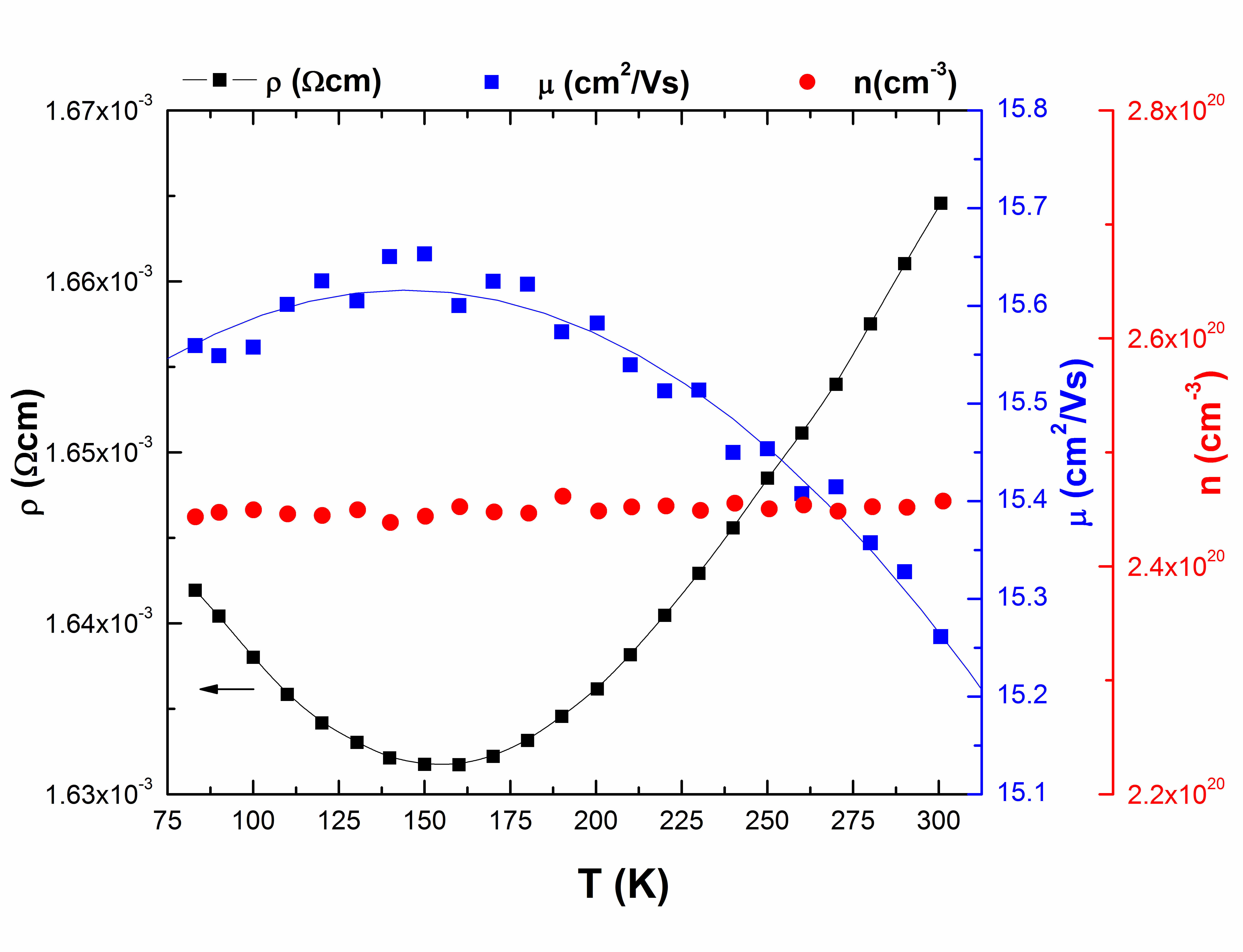
Largely oxygen deficient ITO and In2O3 thin films grown by PED and PLD lead to the synthesis of nanocomposite films, i.e. metallic (In, Sn) clusters embedded in a stoichiometric and crystalline oxide matrix. The presence of these metallic clusters induces a metallic conductivity via percolation with a superconducting transition at low temperature (about 6 K) and the melting and freezing of the In-Sn clusters in the room temperature to 450 K range evidenced by large changes in resistivity and a hysteresis cycle.

Transparent thin film transistors (TTFT)   

Field effect TTFT were fabricated on glass and on low-cost paper substrates. In2O3 and ZnO and transparent thin films, either channel or conducting electrodes, were grown by PED in the classical approach or by self-assembled source-channel-drain structures in a single deposition process with a shadow mask.